
IEEE Boston Section

 This long-running IEEE Course has been updated to include Jupyter Notebooks which incorporates graphics together with Python simulation code to provide a “take-it-with-you” interactive user experience. No knowledge of Python is required but the notebooks will provide a basic framework for proceeding with further signal processing development using that tools for those that have interest in doing so. This course will not be teaching Python, but using it for demonstration. A more detailed course on Python itself is covered in a separate IEEE Course “Python Applications for Digital Design and Signal Processing”. Students will be encouraged but not required to load all the Python tools needed, and all set-up information for installation will be provided prior to the start of class. Target Audience: All engineers involved in or interested in signal processing applications. Engineers with significant experience with DSP will also appreciate this opportunity for an in-depth review of the fundamental DSP concepts from a different perspective than that given in a traditional introductory DSP course. Benefits of Attending/ Goals of Course: Attendees will build a stronger intuitive understanding of the fundamental signal processing concepts involved with digital filtering and mixed signal analog and digital design. With this, attendees will be able to implement more creative and efficient signal processing architectures in both the analog and digital domains. The knowledge gained from this course will have immediate practical value for any work in the signal processing field. Topics / Schedule: Pre-recorded lectures: (3 hours each) will be distributed Friday prior to each week’s workshop dates. Workshop/Q&A Sessions are 6 – 7:30PM on the dates listed below. Kick-off / Orientation: Thursday, April 18, 2024 Class 1: April 25, 2024: Correlation, Fourier Transform, Laplace Transform Class 2: May 2, 2024: Sampling and A/D Conversion, Z –transform, D/A Conversion Class 3: May 9, 2024: IIR and FIR Digital filters, Direct Fourier Transform Class 4: May 16, 2024: May Windowing, Digital Filter Design, Fixed Point vs Floating Point Class 5: May23, 2024: Fast Fourier Transform, Multi-rate Signal Processing, Multi-rate Filters
 Speaker’s Bio: Dan Boschen has a MS in Communications and Signal Processing from Northeastern University, with over 25 years of experience in system and hardware design for radio transceivers and modems. He has held various positions at Signal Technologies, MITRE, Airvana and Hittite Microwave designing and developing transceiver hardware from baseband to antenna for wireless communications systems. Dan is currently at Microchip (formerly Microsemi and Symmetricom) leading design efforts for advanced frequency and time solutions. For more background information, please view Dan’s Linked-In page at: http://www.linkedin.com/in/danboschen Registration is open through the last live workshop date. Live workshops are recorded for later use.
 Consultants’ Network
Consultants’ Network: https://boston-consult.org
Free Dinner starts at 6:00 PM
Meeting starts at 7:00 PM – On-site and Zoom
Members in good standing are encouraged to attend. If you are unable to attend, then we will also be on Zoom.
Your registration confirmation email contains the Zoom details.
As a group of skilled consultants associated with IEEE Boston Section, CNET offers high value professional services for a diverse audience.
For CNET members:
- Professional interactions with peers in a supporting environment.
- General information from insiders about the condition of industry.
- Practical information exchanges about consulting practice.
- Communication improvement across multiple specialties.
- Participation in info-professional events on themes of interest.
- Opportunity to give presentations and hone speaking effectiveness.
- Credibility and visibility within the engineering and technology development community as an IEEE associated consultant.
For engineers interested in becoming consultants:
- Basic information on consulting practice requirements.
- Participation in events and idea exchanges with industry peers.
- Access to established consultants in the area for mentoring.
- Opportunities for improving professional communications skills.
For enquirers on CNET services:
- Convenient access to local consultants with multi-disciplinary expertise.
- Opportunities to enter into consulting agreements without agency fees.
- Direct, easy connection with consultants over the CNET web page.
- Dealing with consultants with multi-year experience validated by IEEE.
Join us!
COURSE DESCRIPTION
Course Kick-off / Orientation Thursday, April 18, 6:00PM – 6:30PM.
Live Workshops: 6:00PM – 7:30PM, Thursdays, April 25, May 2, 9, 16, 23
Registration is open through the last live workshop date. Live workshops are recorded for later use.
Attendees will have access to the recorded session and exercises for two months (until July 23, 2024) after the live session ends!
Speaker: Dan Boschen
IEEE Member Fee (by April 11th): $190.00
IEEE Member Fee (after April 11th): $285.00
IEEE Non-Member Fee (by April 11th): $210.00
IEEE Non-Member Fee (after April 11th) $315.00
Decision to run/cancel course: Friday, April 12, 2024
COURSE DESCRIPTION
New Format Combining Live Workshops with Pre-recorded Video
This is a hands-on course providing pre-recorded lectures that students can watch on their own schedule and an unlimited number of times prior to live Q&A/Workshop sessions with the instructor. Ten 1.5 hour videos released 2 per week while the course is in session will be available for up to two months after the conclusion of the course.
Course Summary
This course is a fresh view of the fundamental and practical concepts of digital signal processing applicable to the design of mixed signal design with A/D conversion, digital filters, operations with the FFT, and multi-rate signal processing. This course will build an intuitive understanding of the underlying mathematics through the use of graphics, visual demonstrations, and applications in GPS and mixed signal (analog/digital) modern transceivers. This course is applicable to DSP algorithm development with a focus on meeting practical hardware development challenges in both the analog and digital domains, and not a tutorial on working with specific DSP processor hardware.
Now with Jupyter Notebooks!
This long-running IEEE Course has been updated to include Jupyter Notebooks which incorporates graphics together with Python simulation code to provide a “take-it-with-you” interactive user experience. No knowledge of Python is required but the notebooks will provide a basic framework for proceeding with further signal processing development using that tools for those that have interest in doing so.
This course will not be teaching Python, but using it for demonstration. A more detailed course on Python itself is covered in a separate IEEE Course “Python Applications for Digital Design and Signal Processing”.
Students will be encouraged but not required to load all the Python tools needed, and all set-up information for installation will be provided prior to the start of class.
Target Audience:
All engineers involved in or interested in signal processing applications. Engineers with significant experience with DSP will also appreciate this opportunity for an in-depth review of the fundamental DSP concepts from a different perspective than that given in a traditional introductory DSP course.
Benefits of Attending/ Goals of Course:
Attendees will build a stronger intuitive understanding of the fundamental signal processing concepts involved with digital filtering and mixed signal analog and digital design. With this, attendees will be able to implement more creative and efficient signal processing architectures in both the analog and digital domains. The knowledge gained from this course will have immediate practical value for any work in the signal processing field.
Topics / Schedule:
Pre-recorded lectures: (3 hours each) will be distributed Friday prior to each week’s workshop dates. Workshop/Q&A Sessions are 6 – 7:30PM on the dates listed below.
Kick-off / Orientation: Thursday, April 18, 2024
Class 1: April 25, 2024: Correlation, Fourier Transform, Laplace Transform
Class 2: May 2, 2024: Sampling and A/D Conversion, Z –transform, D/A Conversion
Class 3: May 9, 2024: IIR and FIR Digital filters, Direct Fourier Transform
Class 4: May 16, 2024: May Windowing, Digital Filter Design, Fixed Point vs Floating Point
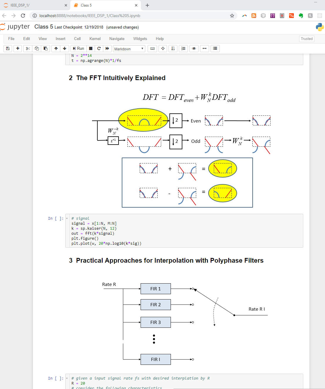
Class 5: May23, 2024: Fast Fourier Transform, Multi-rate Signal Processing, Multi-rate Filters
Speaker’s Bio:
Dan Boschen has a MS in Communications and Signal Processing from Northeastern University, with over 25 years of experience in system and hardware design for radio transceivers and modems. He has held various positions at Signal Technologies, MITRE, Airvana and Hittite Microwave designing and developing transceiver hardware from baseband to antenna for wireless communications systems. Dan is currently at Microchip (formerly Microsemi and Symmetricom) leading design efforts for advanced frequency and time solutions.
For more background information, please view Dan’s Linked-In page at: http://www.linkedin.com/in/danboschen
Registration is open through the last live workshop date. Live workshops are recorded for later use.
Photonics Society
Speaker: Dr. Amos Meeks
Irradiant seeks to unlock the full potential of truly 3D optics and nanophotonics. We achieve this through two fundamental innovations: first, by using two-photon lithography to pattern material within a 3D nanoporous scaffold, we are able to pattern arbitrary 3D gradients of refractive index with index contrast up to 0.6 with <50 nm features. Second, we have achieved two-photon lithography throughputs thousands of times faster than existing systems through a combination of novel two-photon chemistries and a line-scanning DLP configuration. This ultra-high throughput facilitates the cost-effective manufacturing of parts at volumes exceeding millions per year. This enables the same platform to be used for small-scale prototyping and testing through to high-volume manufacturing. To date we have fabricated several novel demonstrations of 3D devices that could not otherwise be made, including multi-layered metalenses, nanoscale free space optics, and more. In addition to passive dielectric materials, we have also demonstrated nanoscale patterning of conductors, quantum dots, and biomolecules, paving the way for future applications in more active and advanced applications.
Bio: Amos Meeks is the co-founder and Chief Technology Officer at Irradiant Technologies, where he works to commercialize a cutting-edge process for patterning large refractive index gradients in complex 3D geometries with nanoscale resolution. In 2021 he received a Ph.D. in Applied Physics from Harvard University in the lab of Joanna Aizenberg, where he conducted research on light-responsive hydrogels as nonlinear optical materials. He received a Bachelor’s degree in engineering from Olin College. His other experiences span a wide range of entrepreneurship, engineering, and materials science.
IEEE Aerospace and Electronic Systems Society – co-sponsored by AESS Boston (Chair Dr. Francesca Scire-Scappuzzo) and AESS London (Chair Dr. Julien Le Kernec)
Seminar: Via formal verification
Speaker: Prof. Alessio Lomuscio, PhD, Imperial College, London, UK. Safe AI Lab. Royal Academy Engineering Chair in Emerging Technologies.
Bio:Dr. Lomuscio is Professor of AI Safety and Director of the Safe AI Lab, Department of Computing, Imperial College London, UK. He is founding co-director of the UKRI Doctoral Training Centre in Safe and Trusted Artificial Intelligence. Alessio’s research interests concern the development of verification methods for artificial intelligence. Since 2000 he has pioneered the development of formal methods for the verification of autonomous systems and multi-agent systems, both symbolic and ML-based. He has published over 200 papers in leading AI and formal methods conferences and journals. He is distinguished ACM member, a Fellow of the European Association of Artificial Intelligence and currently holds a Royal Academy of Engineering Chair in Emerging Technologies. Prof. Lomuscio is the founder and CEO of Safe Intelligence, a VC-backed Imperial College London spinout helping users build and assure robust ML systems.
A major challenge in deploying ML-based systems, such as ML-based computer vision, is the inherent difficulty in ensuring their performance in the operational design domain. The standard approach consists in extensively testing models for inputs. However, testing is inherently limited in coverage, and it is expensive in several domains. Novel verification methods provide guarantees that a neural model meets its specifications in dense neighborhood of selected inputs. For example, by using verification methods we can establish whether a model is robust with respect to infinitely many lighting perturbations, or particular noise patterns in the vicinity to an input. Verification methods can also be tailored to specifications in the latent space and establish the robustness of models against semantic perturbations not definable in the input space (3D pose changes, background changes, etc). Additionally, verification methods can be paired with learning to obtain robust learning methods capable of generating models inherently more robust than those that may be derived with standard methods. In this presentation I will succinctly cover the key theoretical results leading to some of the present ML verification technology, illustrate the resulting toolsets and capabilities, and describe some of the use cases developed with our colleagues at Boeing Research, including centerline distance estimation, object detection, and runway detection. I will argue that verification and robust learning can be used to obtain models that are inherently more robust and better understood than present learning and testing approaches, thereby unlocking the deployment of applications in the industry.
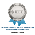
IEEE Boston Section recognized for Excellence in Membership Recruitment Performance
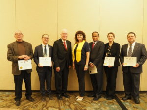
IEEE Boston Section was founded Feb 13, 1903, and serves more than 8,500 members of the IEEE. There are 29 chapters and affinity groups covering topics of interest from Aerospace & Electronic Systems, to Entrepreneur Network to Women in Engineering to Young Professionals. The chapters and affinity groups organize more than 100 meetings a year. In addition to the IEEE organization activities, the Boston Section organizes and sponsors up to seven conferences in any given year, as well as more than 45 short courses. The Boston Section publishes a bi-weekly newsletter and, currently, a monthly Digital Reflector newspaper included in IEEE membership.
The IEEE Boston Section also offers social programs such as the section annual meeting, Milestone events, and other non-technical professional activities to round out the local events. The Section also hosts one of the largest and longest running entrepreneurial support groups in IEEE.
More than 150 volunteers help create and coordinate events throughout the year.